

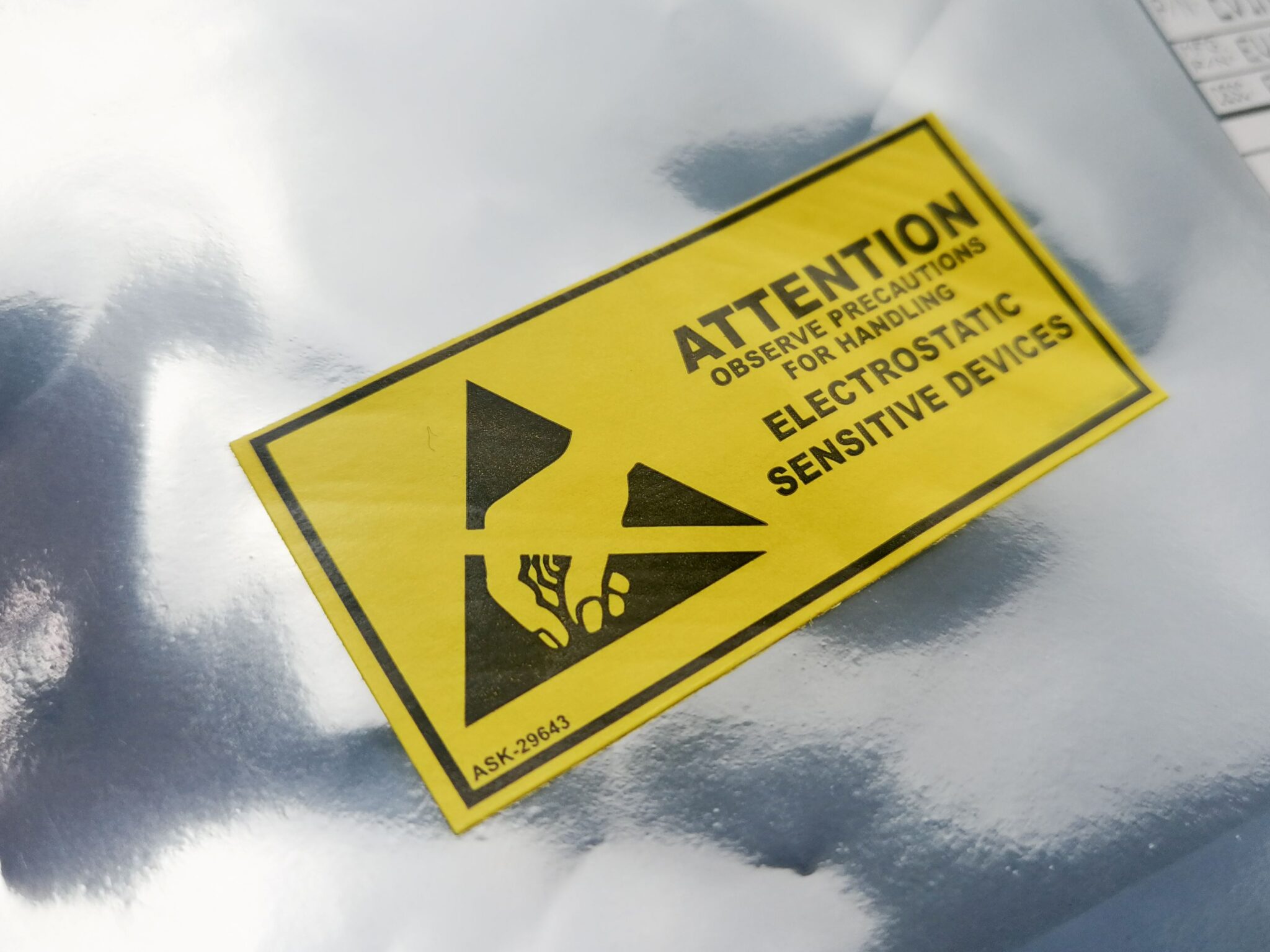
Research Delay via Unpredictable PCBA Failure (ESD-electrostatic discharge)
It can be exasperating to discover that important research results have not been delayed by error in development but rather electronics failure (PCBA ESD electrostatic discharge problems). ESD is essentially random and leaves no evidence or symptom that it has occurred.
ESD has an insidious property that dictates that failure doesn’t necessarily occur immediately. It either immediately destroys electronic chips or introduces premature failure.
There is no cure for it other than preventive measures, on which this article provides guidance. The EM can facilitate full implementation of ESD preventive measures. Please Contact Us if this or advice is required.
What is Electrostatic Discharge (ESD) in relation to PCBAs and Electronics?
The earth’s atmosphere can become charged with electricity as can humans. Most of us know it from the painful experience of discharge, usually through a finger tip which is laced with sensitive nerve endings. The voltages that can be reached are high – in extreme cases up to 15kV. These voltages and charges punch holes in and destroy electronics (PCBs) if discharge takes place through them. The topic is relatively complex and outside the scope of this article, but if greater detail is required, the EM’s article on the Technical Mechanisms of ESD: an Explanation can be read by following the link.
The two mechanisms by which ESD attacks electronics both involve humans. Either a human being has become charged via friction, usually through clothing, or the human is a conduit for discharge of atmospheric electrostatic charge.
So, in short, the manner in which humans handle bare PCBAs (assembled printed circuit boards) can cause premature or catastrophic failure:
- Such handling must be controlled.
- ESD damage is essentially invisible and random.
Why is ESD (electrostatic discharge a problem) for R & D?
The problem is really quite straightforward:
- ESD destroys electronics, sometimes immediately but often insidiously by manifesting itself as premature failure.
- This damage occurs through handling methods and equipment (the following section outlines how it can be substantially overcome).
- Contact Us to learn how these problems may be overcome in your laboratories.
How can R & D avoid Blind Alleys from ESD related (PCBs-electronics) failure? What is the Solution?
The solution lies in taking the following actions:
- Set up ESD controlled areas for testing and handling of bare electronic PCBAs
- Purchase the right equipment, which varies depending on the level of control required, e.g., the handling of ASICs requires equipment and control way beyond the levels of those required for handling of orthodox PCBAs.
- Train everyone involved such that there is general understanding of the problem and how it may be avoided.
- There are ISO standards, e.g., ISO 10605, that cover the requirements, but strict adherence to them may not be necessary: the R & D environment doesn’t require the same vigilance as Operations/Production, usually.
Please Contact Us by pressing the link below if you wish to discuss your requirements or simply need more explanation.