

Is Electronics Development about to be turned on its head?
A Daily Telegraph article (31/12/2025) stated:
‘Britain needs vision. We led the first Industrial Revolution and are nowhere in the fourth.’
This topic reflects this assertion exactly. It is an opportunity not to be nowhere during the fourth Industrial Revolution.
The traditional market model for electronics design followed by manufacture (PCBs and PCBAs) is destined to become a shrinking market. Direct design of ASICs is the future, and most developers and manufacturers in Britain are woefully unprepared for it. This is an old argument that has been reasonably rebuffed in the past, but the circumstances have changed. Asia is doing ASIC from scratch, at low cost and in prototype quantities. Western companies that don’t take heed risk being left out in the cold. Explanations follow for this shocking statement, but electronics design/developers and manufacturers (CEMs) would be well advised to carefully analyse their business plans.
What do many engineers and manufacturers think about ASIC development?
The traditional viewpoint, particularly among the experienced, is that ASIC development is cripplingly expensive and only worth considering when accompanied by a significant budget (£millions) and a need for very high quantities.
Until a few years ago this was true – it isn’t anymore.
Manufacturers (CEMs – contract electronics manufacturers) typically have the same viewpoint.
Why Upskill to doing ASIC from scratch (AfS)?
Let’s first consider what ASIC from Scratch, AfS, is. If we follow the path of a traditional electronics development from low to high volume, the following items illustrate the main stages and outputs:
- Design and development of a PCBA/s that satisfies the technical and commercial specifications resulting in a relatively high cost per item and physically large product.
- Production and sale of the PCBA in question in moderate quantities.
- Commercial success, i.e., higher volume, dictates the need to move to ASIC technology. The previous design is likely useless. The whole system is re-designed from scratch to suit ASIC development.
- A fabrication development process is undertaken. On success, the product is orders of magnitude cheaper and smaller. The process opens opportunities that would have been denied traditional discrete component development – wearable technology, AI, etc.
Most developments never get beyond stage 2 above. They are far from unsuccessful but rather trapped and capped by their design routes.
ASIC from Scratch, AfS, is practicable for all development teams cutting out stages 1 and 2 completely. This is a relatively recent development.
AfS isn’t necessarily the right choice for two reasons. Developing to stage 2 above will cost less (rough factor of 1/3 – detail dependent) and some developments just don’t need the advantages AfS brings, but most do.
How practicable is economic ASIC development from scratch?
The quick answer is it is within the grasp of all design consultancies and manufacturers, but both may need to upskill significantly.
Design
- Engineers will need to become ASIC design capable. This is demanding but well within the capability of experienced electronics engineers.
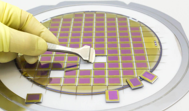
- Wafers, as shown in the main image, containing chip dies will need to be produced. Engineers will need to have some knowledge of wafer fabrication and dicing, but the incredible complexities of making wafers are fortunately covered by the silicon foundry.
- Design is definitely more involved than is the case for standard discrete component circuits. It does involve more iterations, but it isn’t beyond capable electronics engineers.
Companies intending to cover this must ensure their electronics design engineers have training and are comfortable with the ASIC design process.
Manufacture (CEMs)
Electronics designers don’t actually need CEM’s to do anything. The manufacturing resources needed for designers to do AfS are already present. CEMs would be wise to consider what will happen to their market if the AfS development model takes off. There will always be a need for PCBs and PCBAs but AfS will lead to far fewer components and very much reduced PCB size. This could have the following knock-ons for CEMs:
- Very much reduced revenue unless overall demand increases very significantly
- Race to the bottom because the CEM supply will greatly exceed demand unless demand for electronics increases many fold.
- Pick and place machines will become semi-redundant. The need to place many chips quickly will be reduced because component counts will reduce significantly.
- An author’s observation is that the CEM providers have generally invested heavily in the most modern, high volume, PCBA assembly production, test, and inspection equipment. Arguably, the money would have been better spent on increasing the scope of activity to suit AfS than modernising equipment in a market that may yet shrink.
Why is there a change in availability of ASIC development now compared to previously?
The short answer is improvements in technology. Formerly, the engineers view detailed above was essentially true because design and production were complex and suffered from failure (low yield). Experience and improvements in technology have dramatically improved this such that much greater packing densities are now possible, and the packing densities of yesteryear are now high yield, cheap, and available to SMEs.
What could be the consequences of disregarding this article?
The following are the risks to the existing infrastructure if AfS becomes widespread:
There could be consequences for the entire electronic product development and supply chain. CEMs (contract electronics manufacturers) may be facing a shrinking market and unable to capture the up and coming market for want of investment in the right processes. Design consultants and electronics design departments face having teams unable to design electronics meeting the current standards coming from the far east. More detail follows in the bullets below:
- CEMs (contract electronics manufacturers): the author has witnessed very significant investment in this sector. Typical areas of investment are in the most modern PCBA volume, assembly equipment and inspection of the same. This is configuring for a market that will shrink if AfS takes off. It would be better to increase the scope of manufacture such that ASIC technology can be manufactured, leaving wafers to expert suppliers, but covering the other major elements of the supply chain. This leads to a widening of the necessary bandwidth of supply such that the potential electronics revolution is covered. CEMs should consider introducing die and flip chip bonding along with chip packaging.
- ASIC Design: design of electronics and the integrated circuit level is a skill in itself, but it is one experienced and qualified electronics engineers are well suited to. Design consultancies and engineering teams should configure training and or recruitment to cover these skills. This involves: design training, software CAD use, and a reasonable level of training in the fabrication process as a minimum.
- Component Distributors, e.g., Avnet, Anglia (Distis): there are profound changes in the skills Distis will need serve the market. Currently standard chips are proffered and supported, but this will no longer be the main thrust. Presumably licences to use die designs will be sought, and IC supply will be replaced by wafer supply. It is difficult to know exactly what will happen for Distis, but the current offering would not fit if the AfS (ASIC from scratch) model became widely adopted.
A closing note that is food for thought, the issue of producing ASICs from scratch is pretty much essential for Edge AI.
Ever more power and storage in the tiniest spaces will be required to best deliver the performance that AI requires, and ASIC development is a fundamental requirement if Edge AI is the goal.
Should you wish to know more or want to comment on this article please don’t hesitate to contact us.