

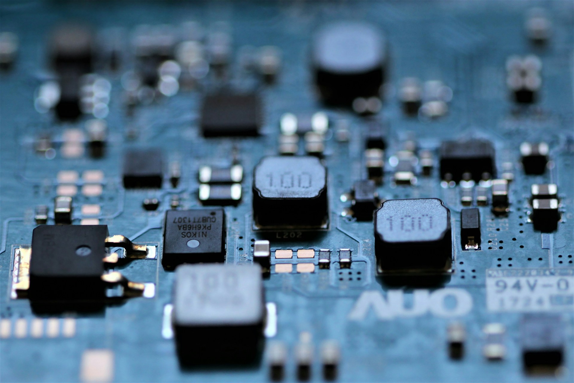
RF PCB Design to usher in AI
Maximal performance from electronics (PCBs) to provide bandwidth for computation will demand ever more of PCB and IC design. RF (radio/high frequency) design of PCBs is at times very challenging: a fact it would be arrogant not to accept, but are some RF PCB designers guilty of setting up smokescreens and claiming a clockmaker’s precision whilst wielding a hammer?
Why is RF PCB Design even more critical than it was pre-AI?
It is all to do with the ever greater demands AI is going to make of memory and speed? Certain types of AI require excessive levels of data storage and computation: and the latter requires speed. Speed in the world of electronics boils down to frequency. Roughly stated, the higher the frequency a computational system is capable of the faster it can be.
As AIoT evolves, ever quicker speeds will be demanded of circuits on PCBs. PCBs will need to be designed to the very limits of the performance their materials, components and construction can achieve. AI is a wonderful technological evolution, but it carries with it the millstone of requiring the very fastest speeds PCB technology is capable of.
PCBs will need to be designed to the limits their materials and construction will allow.
What difference does RF (high frequency) make to PCB Design?
The process of designing a PCB, or any other product to be used for high frequency communications, boils down to a few simple concepts (despite actually designing being very complex):
- Attenuation – loss in amplitude of signals as they pass over the channel (PCB). This is not volt drop in the power sense! More complex.
- Delay – at high frequencies signals are delayed. If tracks are of different lengths, signals arrive at different times.
- Impedance – this is difficult to explain because it isn’t the impedance seen from a circuit designer’s point of view. It is a property of an assembly that derives from its dimensions and materials (complex formulas).
To achieve a given performance, assuming all the components on the board are capable and layouts are not prone to electronic noise, becomes a problem of dimensions and materials with the right properties. The dimensions must be precise otherwise impedance is fouled, and materials, particularly the insulating ones, must have the right properties.
Designing a high frequency PCB correctly means the following during its construction:
- Accurate placement and dimensioning of tracks
- Careful design of the PCB layer stack such that the distances between the different copper areas that form a transmission line are accurate.
- Careful choice of the base material of the PCB such that it has wideband electrical stability (most particularly the relative permittivity remains stable over the bandwidth and temperature range of use).
- Matching of impedance (needs all the above) at source and destination.
Why is high frequency PCB Design occasionally crude? What’s to be done about it?
The best way to illustrate this point is by the exemplar of another industry that has been designing using sound principles for the best part of a century.
The electric cable industry is the exemplar in question. It might be presumed that it has very much less in the way of dimensional problems to contend with, but that would be wrong.
For those in the know, try working out the primary and secondary constants for a multipair cable with only a collective screen!
High frequency cables typically use materials like polythene for insulation. This material has incredibly stable electrical performance – if PVC were used, high frequency cables would vary by batch, frequency, and temperature. The right material for the task is invariably chosen by cable makers. High frequency cables are also designed and manufactured to precise dimensions. The result is cables generally have predictable and stable high frequency performance characteristics.
So, what’s the situation with high frequency RF PCB design? Unfortunately, not as good:
- Understanding how to design PCBs or cables requires a deep understanding of transmission lines. Electronics graduates usually study and forget this. It is crucial that the cobwebs are brushed off it for grade one high frequency design. The author’s experience is that there isn’t deep understanding generally.
- The materials used for PCBs vary, but the only one that is a true high frequency contender is PTFE, which is rarely used. The most common material is epoxy (glass reinforced or Rogers material). Epoxy doesn’t have stable relative permittivity, especially as the glass temperature is reached. Typically, the materials used in PCBs have properties that change depending on the direction of travel of an electromagnetic wave. Despite, with the exception of PTFE, the materials used in PCBs being inferior to those used in other related designs, the errors introduced are not as problematic as those introduced via dimensions.
- Effort is usually expended on designs to ensure PCB tracking is correct for impedance matching, but the components that are used to terminate the tracks and the impedance matching at chip pins, are often not properly accounted or over-looked.
This article has only scratched the surface of this topic but:
It is clear that high frequency PCB design has a long way to go to properly service the AI revolution.
The EM has a lifetime’s experience developing designs for use in high frequency environments. This is primarily for PCBs, but cables, installations, and fibre optics are all in its gift. Please feel free to contact us.