

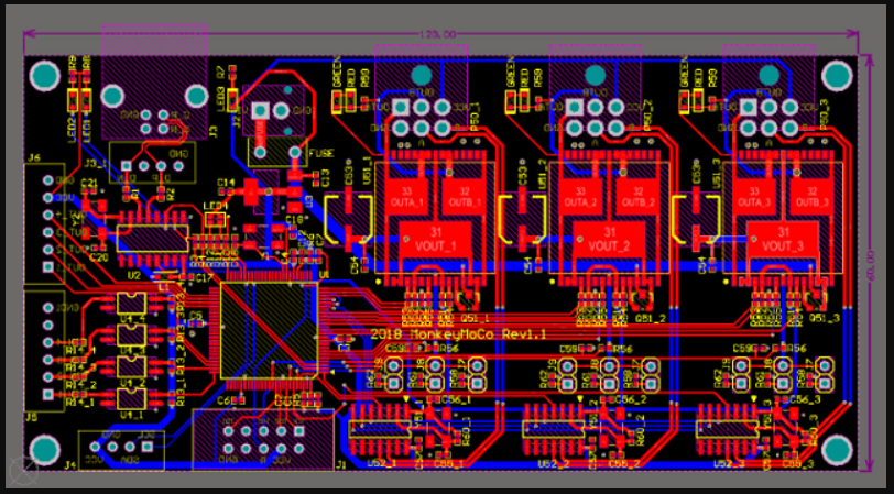
PCB Layout: explanation and service
The EM’s clients sometimes have an effective design: they just need PCBs designing. The EM is happy to undertake such work that usually entails one of the following EM core skills:
- RF design and/or high layer numbers
- Design for manufacture and test
- CEM (contract electronics manufacturer) management
- Shoehorn layouts – PCB miniaturisation
- Reverse Engineering
Please note that some unscrupulous suppliers attempt to go through a PCB layout process and then withhold the design file (IP in effect). The EM does not do this. Read the ‘design blackmail’ article for more detail on this.
RF Design and intricate PCB Layout
The EM has experience of designing PCBs for use at 1GHz and above. The advent of AI and moves towards ASIC designs will usher in a period during which PCBs will be pushed to their physical limits – ever more performance will be demanded of lower and lower PCB real estate.
It is a fact that despite RF design of PCBs being pushed to the fore by the marketplace, the methods and materials used in the industry lag other product markets, e.g., RF cables. If this topic interests you feel free to read the RF Article (link) on it.
Complex layout is withing the EM’s gift. Please feel free to Contact Us if you have such a requirement.
Design for manufacture, test, and/or service
The principle staff of the EM are all time served in PCB fabrication and PCBA assembly. Problems such as copper deserts, heavy components on both sides of and SMD PCB, and failure to implement sufficient thermal relief are problems the EM never introduces, along with the plethora of other issues that apply to PCB fabrication and assembly.
It is necessary to functionally test boards that have just been through a re-layout, and because the EM is a design consultancy we are able to service this. We can also assist with the design of functional testing if it is required.
CEMs (contract electronics manufacturers)
The presence in the electronics marketplace is such that we can source CEMs to suit any given client. We also, if required, will manage a CEM. Manufacture of electronics is an arcane topic, and many CEMs don’t shield their clients from this. The EM is more than happy to smooth such communications.
Shoehorn PCB layout (PCBA miniaturisation)
The marketplace is changing with regard to miniaturisation (see ASIC article), but there remains a need to layout PCBs on minimal real estate to both facilitate miniaturisation and reduce RF issues. The EM is well placed to take on such developments.
Reverse engineering of existing designs
Reverse engineering can be undertaken by the EM, but we would point out that it is usually an opportunity. Companies that approach us for reverse engineering are often over a barrel for one reason or another, and this can lead to a minimalist approach that requires only a return to the status quo. It is an usually an opportunity to leap frog the status quo and take the product to its next evolution.
Should you wish to know more or want to comment on this article please don’t hesitate to Contact Us.